

Hints on Effective Cooling of High-Power PCBs
August 27, 2026
Heat poses a real threat to the longevity and reliability of any electrical circuit. When subjected to excessive thermal stress, PCB materials and power components can drift outside the operating conditions they were designed for. Consequently, thermal management becomes a critical consideration when designing PCBs that incorporate high-power devices.
For this reason, the board’s maximum operating temperature and each component’s power consumption must be evaluated before a new PCB design begins. Defining the layout and positioning components appropriately are the first two steps toward establishing an effective heat-dissipation path away from high-power devices.
Because boards densely populated with high-power components are especially prone to overheating, careful design must guard against the following consequences of excessive, unmanaged heat:
- Breakdown of the PCB’s dielectric and substrate materials
- Damage to conductive traces (partial or complete burning)
- Separation of solder joints from the underlying layer
This article offers practical guidance for designers tackling cooling challenges in PCBs that carry high-power components.
Active and passive cooling
PCB cooling approaches fall into two broad categories: active and passive cooling systems.
Choosing the right method depends on the temperature differential between the board and its operating environment. Passive cooling generally suffices when ambient temperature exceeds the PCB’s working temperature. However, active cooling becomes necessary once heat generated by high-power devices climbs close to their maximum rated temperature.
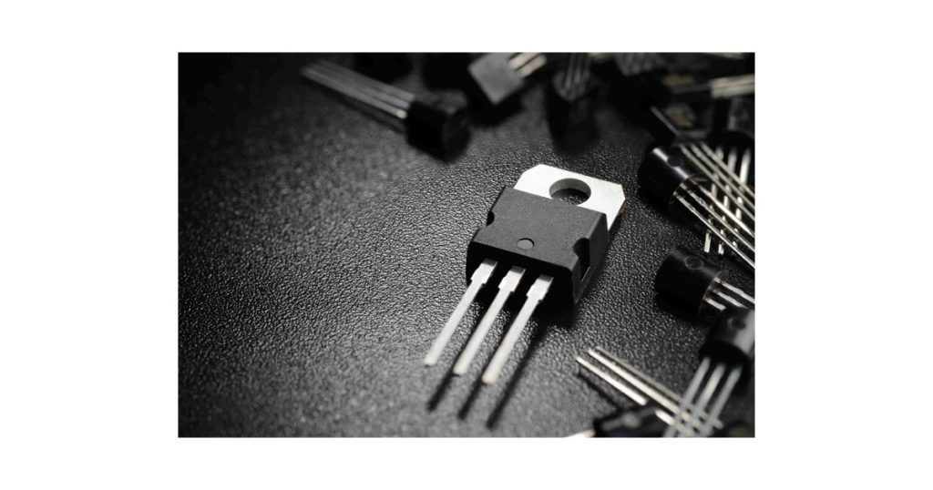
For passive cooling of power components, it’s advisable to use copper areas — typically placed directly beneath the device — to promote even, consistent heat spreading. Many such components are designed with metal tabs to facilitate this (see Figure 1).
That said, the pad beneath the component should not extend beyond its edges. If a single pad can’t bring the temperature down sufficiently, a heatsink mounted on top of the device may be needed. Applying thermal paste or a thermal pad between the device and heatsink is generally recommended to improve heat transfer to the radiator.
In some cases, active cooling is unavoidable. A fan, for example, may be required when passive cooling can’t adequately cool components with heavier current demands — such as FPGAs, GPUs, CPUs, or other active devices switching at high frequencies. The degree of active cooling applied is typically controlled by the fan’s rotational speed, which is adjusted based on die or package temperature readings from a dedicated sensor.
In such cases, the board must be designed with a PWM signal to control fan speed and a sensor to monitor component temperature. Unfortunately, a PWM-driven fan generates radiated electromagnetic emissions at its base switching frequency and associated harmonics. As a result, designs using a fan must either incorporate noise-suppression measures — such as filters or chokes — or keep EMI-sensitive components away from the affected area.
More advanced active cooling techniques, found in high-power amplifiers or high-performance motherboards, rely on circulating coolants (glycol or water) through metal piping to carry heat away from concentrated hotspots.
Selection of the PCB materials
Beyond active and passive cooling techniques, choosing the right materials for PCB layers and substrates is another key factor in achieving strong thermal performance. These materials need to offer better thermal conductivity and more even heat spreading than conventional, lower-cost options.
FR-4, the standard substrate material for typical PCBs, offers poor thermal conductivity. For applications involving high-power components such as MOSFETs or power LEDs, aluminum or metal-core PCBs (MCPCBs) may be a better fit — though these options limit how many layers can be included in the stack-up.
Another approach involves using thicker copper traces for connecting power devices. The tradeoff, though, is that thicker copper makes narrow trace widths harder to achieve, creating trace-spacing constraints in the layout.
Although achieving uniform heat distribution during PCB design takes deliberate effort, designers should steer clear of overly concentrated power — and therefore thermal — zones.
Rules for layout design
By following a handful of core principles during layout design, engineers can effectively manage heat dispersion. Here’s what these guidelines involve.
First, temperature-sensitive components should be positioned in the coolest areas of the board, well away from any cooling hardware.
Depending on the required thermal performance, the board’s main heat sources should be spaced as far apart as possible. Where a cooling fan is present, cooler components should sit upstream of the airflow, while components generating substantial heat or exhibiting high thermal resistance should be placed downstream.
High-heat-producing devices should occupy locations offering the best dissipation potential — for example, kept clear of corners and board edges unless properly heatsinked. Because high-power components are often the primary source of overheating, they should generally sit near the board’s center to allow heat to spread evenly through the circuit.
Likewise, the board’s core is the preferred location for high-power components like processors and microcontrollers. Placing such a component near the board’s edge causes localized temperature spikes and heat accumulation there, whereas centering it allows heat to disperse more evenly across the board’s surface — ultimately lowering the overall surface temperature.
On boards relying on free-convection air cooling, heat-dissipating components such as ICs are best arranged in a longitudinal pattern. Conversely, when forced (active) cooling is used, arranging the same components transversely is the better choice.
Placing thermal vias as close as possible to heat sources is always recommended, as it improves heat conduction and helps spread it over a wider area. Thermal vias channel heat toward the ground planes within the PCB stack-up, helping distribute it evenly across the board. A ground plane positioned beneath signal traces also enhances signal integrity and reduces noise, while doubling as a heat sink.
To draw heat efficiently away from hot components, thermal vias should be placed beneath devices with high or widely fluctuating operating temperatures — for instance, power components like regulators and transistors, or dense logic devices such as CPUs and FPGAs. Designing the vias to maximize contact surface area improves cooling efficiency, an outcome that’s often easier to achieve using arrays of multiple thermal vias.
Solid, continuous ground planes deliver better thermal performance and are essential in any design. They provide a simple yet highly effective way to move excess heat from its source to areas with greater surface area, where it can dissipate less intensely. Using the outer layers as ground planes further boosts heat dissipation by enabling additional convective cooling across a wider region, ideally spanning close to the full board size. Pad shape plays a critical role in thermal management. Since the top copper layer of the pad is where heat is released, it must be thick enough to spread that heat across a wide enough area. Because heatsinks are commonly mounted on the underside of the copper pad, the pad’s cross-section must also be large enough to conduct heat effectively through to the heatsink.